Neil GerrardSenior Editor, Construction Briefing
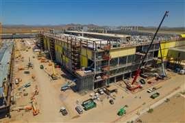
Aerial view of Taiwan semiconductors’ mega factory under construction in North Phoenix, Arizona. (Image: Noah Hairston/Wirestock Creators via AdobeStock)
Geopolitical tensions and stress on supply chains amid the Covid-19 pandemic have highlighted the need for manufacturers to re-shore production or move it closer to home.
That has helped to make industrial and manufacturing projects the hottest area of construction in the world, according to a recent survey.
And there are few areas where the scramble to diversify production is sparking more investment in major new construction projects than when it comes to semiconductor manufacturing facilities (also known as ‘fabs’).
Policy initiatives from the US government and its European counterparts have helped to drive a flurry of investment in the sector, amounting to hundreds of billions of dollars.
The United States of America’s CHIPS and Science Act of 2022 aims to catalyse investment in the domestic semiconductor market, as well as kickstarting more research and development, by offering grant and tax breaks for the construction of new facilities.
The programme is directing $280 billion in spending towards the sector over the next 10 years, with $52.7 billion for manufacturing and $200 billion for scientific research and development and commercialisation.
And the construction of a fab doesn’t come cheap. Chip giant Intel says that a fab, which typically contains 1,200 multimillion-dollar tools and 1,500 pieces of utility equipment, takes about three years and $10 billion to construct.
Intel’s facilities are typically 70ft (21m) tall and spread across four levels: a fan deck on the top level to keep the clean room below particle-free and at the right temperature; the clean room, where production of silicon wafers for computer chips takes place; a clean subfab level full of pumps, transformers and power cabinets that support the clean room; and a utility level where electrical panels that support the fabs along with chillers, compressors, and large utility pipes are located.
Here are some of the biggest semiconductor fabs either under construction or about to start construction:
1) Samsung’s $230 billion semiconductor ‘mega-cluster’, South Korea
South Korean electronics giant Samsung announced earlier this year that it will invest $230 billion over the next two decades, as part of a project to build the world’s largest semiconductor manufacturing base near Seoul.
The ‘mega-cluster’ will be centred around five new Samsung semiconductor plants close to its existing factors.
The move is one of the most high-profile examples of major players in the world of chip making ramping up efforts to boost onshore manufacturing.
But there are few details so far on when construction in Gyeonggi Province will start.
2) $100 billion Micron ‘megafab’, New York, USA
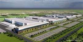
Preliminary illustration of how Micron’s ‘megafab’ in New York, USA, could look (Image: Micron)
Micron, which claims to be the only US-based manufacturer of memory announced in October last year that it would invest up to $100 billion in a new ‘megafab’ in Clay, New York.
The first phase of investment, worth around $20 billion and it has been billed as the largest private investment in New York state history.
Micron could eventually build four 600,000 sq ft (55,741 sq m) clean rooms, aided by $5.5 billion in incentives from the state of New York over the lifetime of the project, as well as grants and tax credits from the CHIPS and Science Act.
Site preparation is starting this year before construction begins in 2024.
3) $40 billion TSMC fabs, Arizona, USA
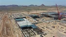
Progress on construction at TSMC’s fab in Arizona (Image: TSMC)
Taiwan Semiconductor Manufacturing Company (TSMC) is building two fabs in Phoenix, Arizona.
Originally, it planned the construction of just one fab, investing $12 billion, but announced in December 2022 that it would build a second and would more than triple its investment to $40 billion.
The project is expected to create over 10,000 construction jobs and represents one of the largest foreign direct investments in US history.
Taiwanese contractor CTCI is providing engineering, procurement and construction (EPC) services via an Arizona subsidiary. Arizona-based Okland Construction Company, and Marketech International Corp are also involved in the project. United Integrated Services is delivering the mechanical, electrical and plumbing (MEP) services and clean room construction services.
The first fab was due for completion in 2024, with the second originally due start production in 2026. But earlier this summer, TSMC announced that production at the first fab would not start until 2025. It cited shortage of skilled workers with the “specialised expertise required for equipment installation in a semiconductor-grade facility”. It said it was sending specialists from Taiwan with the required expertise to train local workers.
Together, the two TSMC fabs are expected to manufacture over 600,000 wafers per year.
TSMC is also planning an on-site industrial water reclamation plant, which it said would allow the facility to achieve near zero liquid discharge on completion.
4) €30 billion ($33 billion) Intel fab, Magdeburg, Germany
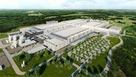
A digital render of Intel’s planned facility in Magdeburg, Germany (Image: Intel)
Intel is making another major investment in Magdeburg, Germany, where it is building a semiconductor ‘mega-fab’.
The project had faced delays amid rising costs, which grew from an initial estimate of $17 billion to a reported $30 billion.
But the project is now set to move ahead after Intel struck a deal with the German government for almost $11 billion in subsidies.
In the initial phase, Intel will build two fabs in Magdeburg, creating 7,000 construction jobs. They will sit on a site of almost 1,000 hectares (2,471 acres), offering space for up to eight connected chip factories.
The European Union has been pushing to develop its own chip manufacturing capability. In April this year, the European Parliament and European Union member states signed the European Chips Act with the aim of boosting the global share of chips manufactured in the region from 10% now to 20% by 2030.
5) $30 billion Texas Instruments fab in Texas, USA
A digital render of Texas Instruments’ factory in Sherman, Texas (Image: Texas Instruments)
Texas Instruments is leading the construction of up to four fabs in Sherman, Texas to produce 300mm semiconductor wafers, destined for all sorts of electronic equipment. The total investment could be as high as $30 billion.
Contractor Austin Commercial broke ground on the project in May 2022 and the fabs will be built to the Leadership in Energy and Environmental Design (LEED) Gold standard.
Production from the first Sherman fab is expected to start in 2025.
Meanwhile, Texas Instruments expects to start construction on a second semiconductor wafer fab in Lehi, Utah, later this year.
Once complete, the $11 billion facility will operate as a single fab alongside the existing plant.
6) $25 billion Samsung factory, Taylor, Texas
Digital render of Samsung’s semiconductor fab in Taylor, Texas (Image: Samsung)
In the US, Samsung is currently building a new semiconductor plant at Taylor, in Texas.
The project was originally expected to cost $17 billion, although that figure has reportedly risen to $25 billion as a result of inflation.
Yates Construction is general contractor on the scheme, which broke ground in 2022 with a targeted completion of 2024.
7) $20 billion Intel facility, Ohio, USA
Engineering and project management company Bechtel is designing and building the first phase of two fabs for Intel in New Albany, Ohio.
Work is already underway, with Bechtel saying the construction would require as much steel as eight Eiffel Towers and as much concrete as the tallest of skyscrapers.
Intel is investing $20 billion in the two chip factories, the construction of which is expected to support around 7,000 construction jobs.
The site in Licking County covers nearly 1,000 acres and can accommodate up to eight fabs in total.
Production at the two new facilities is expected to come online in 2025.
8) $20 billion Intel fabs, Arizona, USA
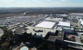
Construction work in progress at Intel’s factory in Arizona (Image: Intel)
Intel is also building two new fabs in Chandler, Arizona at its Ocotillo campus. The project has a price tag of $20 billion and represents the largest private sector investment in Arizona.
Contractors broke ground on Fab 52 and 62, as they are known, in September 2021. They are due for completion in 2024.
Jacobs Engineering is reported to be designing the project with Hoffmann Construction working as general contractor.
The first of 36 steel trusses, each 51m long and weighing 163 tonnes, was lifted into place in October 2022. The project is expected to use 400,000 cu yd (305,822 cu m) of concrete and 40,000 tons of steel.
9) $10.3 billion Nanya chip facility, Taiwan
Taiwanese chip manufacturer Nanya, the fourth largest maker of DRAM memory chips in the world, is building a fab in New Taipei City.
The project has hit delays as a result of regulatory hurdles, shortages of materials, components and construction workers.
The project was originally due to finish by the end of 2023 but is facing a delay of more than six months. It is now due to start production in 2025.

